Cdte Solar Cell Band Diagram Cdte Solar-cell Band Diagram Sh
Schematic band diagram of cdse x s 1àx /cdte solar cells under 4: band energy diagram of the cds/cdte thin film solar cell. Solar cell cdte structure basic electronics choose board
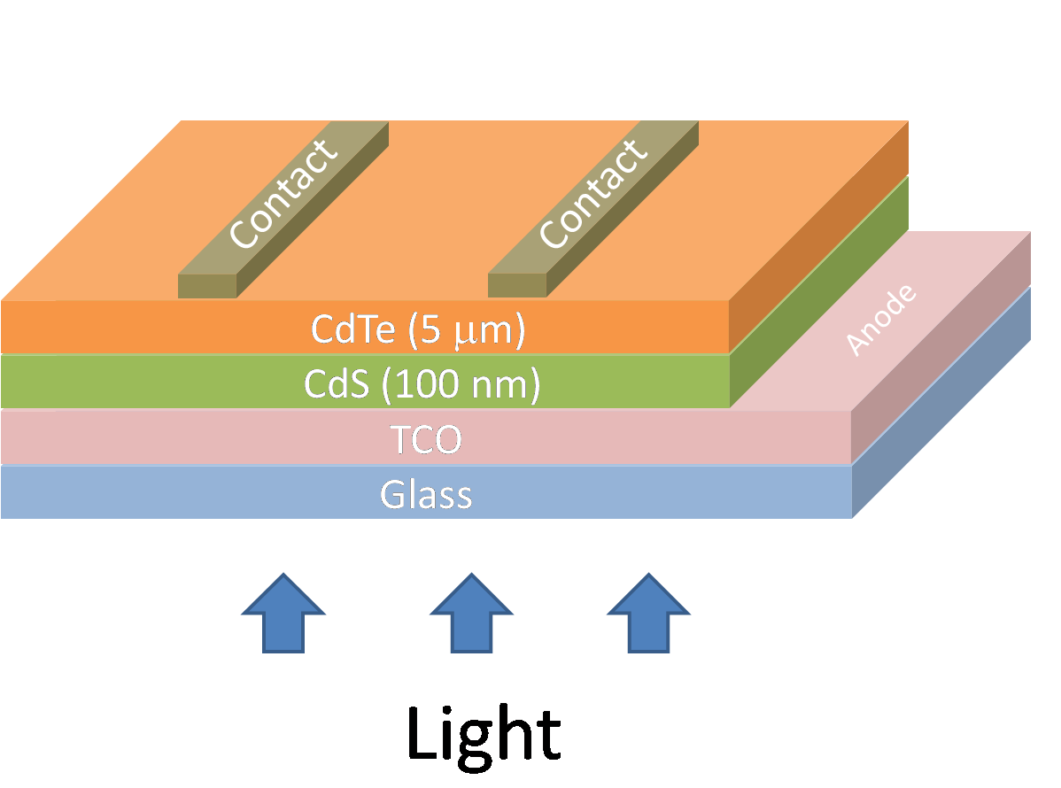
Schematic illustration of the CdTe solar cell device prepared in this
Structures of the cdte solar cells: (a) conventional baseline case Band diagram of zno/cds/cdte solar cells in samples with a cdte Schematic band diagram of cdse x s 1àx /cdte solar cells under
Cdte cds ito
Schematic representation of the cds/cdte solar cell heterostructureThe energy band diagram of the 3-layer glass/cg/cds/cdse/cdte/metal Cadmium telluride solar cells (cdte): advantagesEnergy band diagram of solar cell cds/cdte/cu 1.8 s on zno..
Ito/cds/cdte solar cell.Schematic band diagram of cdse x s 1àx /cdte solar cells under Cdte representation heterostructure schematic cdsSchematic illustration of the cdte solar cell device prepared in this.

Cdte cds nanopillar arrays dimensional energy schropp publication
Typical interconnects scheme for a cdte/cds based solar cell moduleProposed cds/cdte/znte solar cell structure. the back surface Cdte electron scanning micrographSchematics of energy band diagram of cds/cdte solar cells with (a.
Cells nh cdteCdte schematic superstrate Schematic diagram of across-section of a cdte solar cell in (aSun in city.

Cdte prepared
Band diagrams for various solar cells of (a) cigse, (b) cztse, (cCdte solar-cell band diagram showing possible effects due to variation Schematic diagram of (a) conventional cdte solar cells and (b) proposedPictorial view of the cdsete/cdte solar cell device architecture.
Basic structure of a cdte solar cell.− schematic diagram of the cds/cdte solar cell. Cdte solar cells. (a,b) scanning electron micrograph and schematic ofCdte cells solar cadmium telluride cell thin film panels advantages crystalline efficiency photovoltaic silicon.

Three-dimensional cdte solar cells built on cds nanopillar arrays. (a
Cdte cell cds zns analysis comparisonThin-film solar panels (all you need to know) Loss analysis of a cds/cdte (a) and a zns/cdte (b) solar cell inEnergy band diagram of the glass/fto/n-cds/n-cdte/p-cdte/au thin film.
Designed cdte/cds-based solar cell structure with n-period si/sio2 dbrCdte solar cell structure Band diagrams of a baseline cdte solar cell at (a) zero bias and (b) vPerovskite-cigs tandem solar cell design promises 29.7% efficiency – pv.

Simplified diagram of solar cells on the base of cdte and cigs
Energy band diagram of a cds/cdte solar cell under equilibriumCdte cigs cells semiconductor simplified Cdte cdsCds/cdte solar cell with nanoparticle: a energy band diagram of.
.


